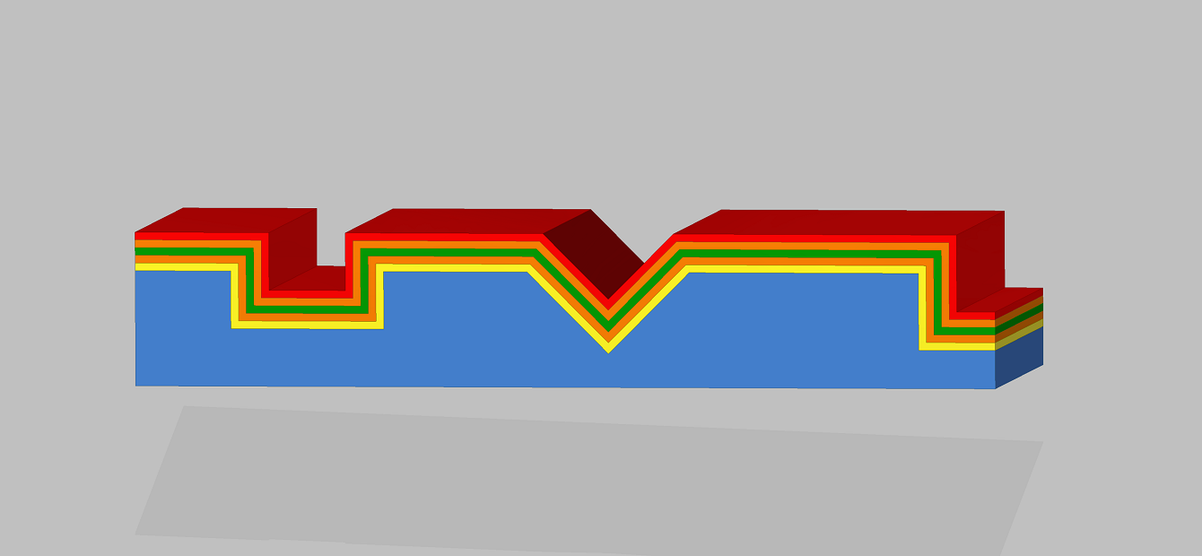
In an all-in-one system, the substrates are applied in any sequence using the thin-film process.
By using a multi-layer sandwich, UV and temperature problems can be improved by several factors.
In addition, the following problems:
are reduced by up to 1000 times due to higher density in the surfaces.
Structured surfaces such as PCBs, wafers and sensors can be coated with this method.
Thanks to our many years of experience in the field of PECVDs and patented thin-film processes, we are happy to advise you.To clarify further technical details, please contact us; we will be happy to consult with you.
If you have any questions about our services and offers, you can use the following form! We will get back to you as soon as possible.